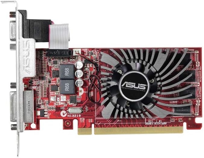
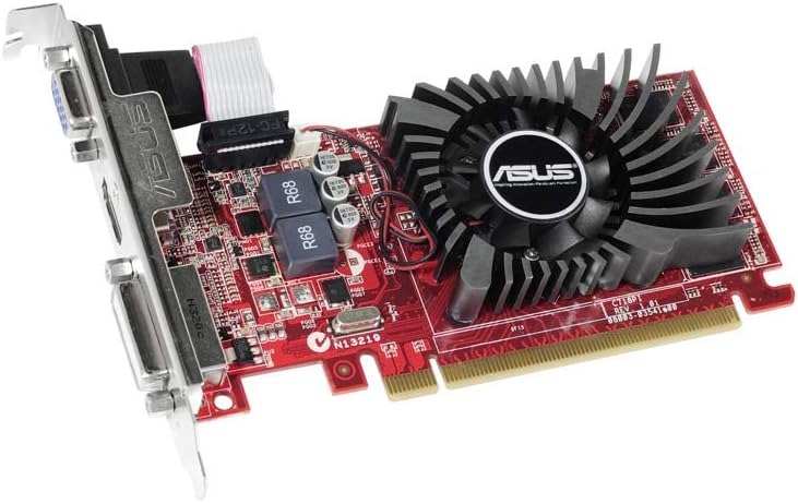
The Oland PRO GPU, part of AMD’s GCN 1.0 architecture under the Volcanic Islands (R7 200) generation, succeeding the Sea Islands and preceding the Pirate Islands architectures. Built using a 28 nm process at TSMC, the GPU packs 950 million transistors on a die size of 77 mm², with a transistor density of 12.3M/mm². The chip package is FCBGA-962.
As a budget-friendly graphics card, the Oland PRO GPU operates over a PCIe 3.0 x8 interface. It comes with base and boost clock speeds of 730 MHz and 780 MHz respectively, along with a memory clock of 900 MHz (effective 1800 Mbps). The card features 2 GB of DDR3 memory over a 128-bit memory bus, offering a memory bandwidth of 28.80 GB/s.
In terms of rendering, the Oland PRO is equipped with 320 shading units, 20 TMUs (Texture Mapping Units), and 8 ROPs (Render Output Units). It also includes 5 Compute Units (CUs) with 16 KB L1 cache per CU and 256 KB of L2 cache. The theoretical performance delivers 6.240 GPixel/s pixel rate, 15.60 GTexel/s texture rate, and 499.2 GFLOPS FP32 (float).
Despite its modest performance, this GPU maintains low power consumption with a TDP of 30W, making it suitable for systems with minimal power needs. It doesn’t require additional power connectors, and its single-slot design measures between 159-168 mm (6.3-6.6 inches) in length, allowing it to fit into compact builds. A 200W power supply is recommended to ensure stable operation.
For connectivity, the card provides 1x DVI, 1x HDMI 1.4a, and 1x VGA outputs, supporting a range of display options. In terms of API support, it is compatible with DirectX 12 (11_1), OpenGL 4.6, OpenCL 2.1, Vulkan 1.2.170, and Shader Model 6.5.
Though now considered end-of-life, the Oland PRO GPU remains a viable option for light workloads and basic gaming at low resolutions.


![NVIDIA GeForce GTX 690 DUAL CHIP [ 2 X 2 GB, GDDR5, 256 X 2 BIT, DX 12 , 1536 X 2 CORES ]](https://i0.wp.com/almasoomtrader.pk/wp-content/uploads/2023/07/images-3.jpeg?fit=252%2C200&ssl=1)
![EVGA NVIDIA GEFORCE GTX 970 [ 4GB, GDDR5, 256BIT, DX12 ] [ BEST FOR GAMING AND GRAPHIC WORK ] GRAPHIC CARD](https://i0.wp.com/almasoomtrader.pk/wp-content/uploads/2023/07/S68ec8219c8ed4c588771eb4953b907e4b.jpg_750x750.jpg_.webp?fit=300%2C294&ssl=1)
![NVIDIA GEFORCE GTX 645 [ 2GB, GDDR5, 128BIT, DX 12 ] [ GAMING GRAPHIC CARD ]](https://i0.wp.com/almasoomtrader.pk/wp-content/uploads/2023/07/bc5242704c9598329f301160f088-removebg-preview.png?fit=430%2C287&ssl=1)
![AMD RADEON R5 430 [ 1GB, GDDR 5, 64 BIT, DX 12 ] GAMING GRAPHIC CARD](https://i0.wp.com/almasoomtrader.pk/wp-content/uploads/2023/07/44232.jpg?fit=430%2C430&ssl=1)
![EVGA GEFORCE GTX 960 [ 4GB, GDDR5, 128 BIT, DX 12 ] GAMING GRAPHIC CARD](https://i0.wp.com/almasoomtrader.pk/wp-content/uploads/2023/07/evga_geforce_gtx_960_4gb_sc_gaming_graphics_card3_-_tejar.jpg?fit=300%2C300&ssl=1)
There are no reviews yet.